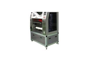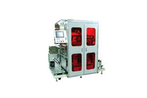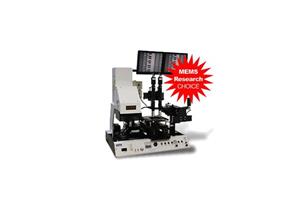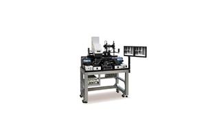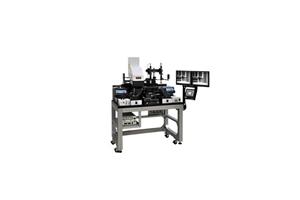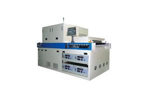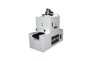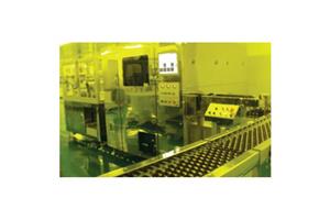
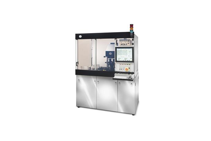
For: Semiconductors, MEMS, Sensors, Microfluidics, IOT, Packaging With over 4 decades of manufacturing in the semiconductor industry, OAI meets the growing challenge of a dynamic market with a new elite class of production photolithography equipment.
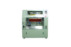
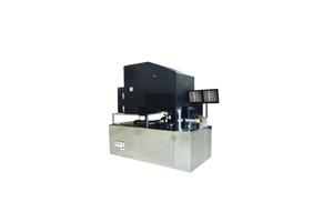
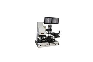
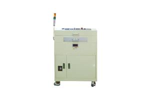
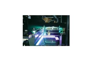
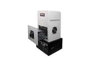
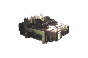
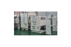
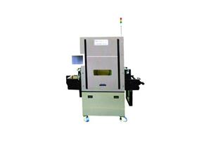
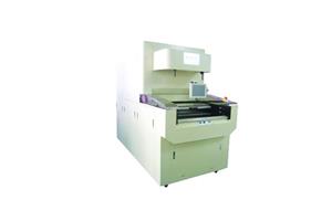
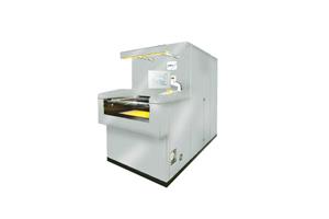
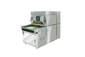
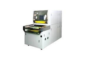
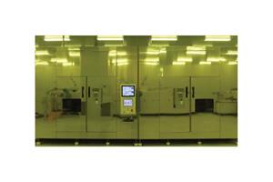
Built on the venerable OAI modular platform, the Series 6000 has topside or backside alignment that is fully automated with sub-micron resolution which delivers performance that is unmatched at any price.
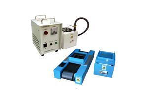
The Aligners have Advanced Beam Optics with better than ±3% uniformity and a throughput of 180 wafers per hour in first mask mode, which results in higher yields. The Series 6000 can handle a wide variety of wafers from thick and bonded substrates (up to 7000 microns), warped wafers (up to 7 mm-10mm), thin substrates (down to 100 micron thick), and thick photo resist.
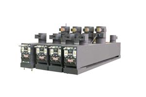
With superb process repeatability, the Series 6000 is the perfect solution for all production enviroments. Choose either top side or optional back side alignment which uses OAI's customized pattern recognition software that is Cognex based. For the total lithography process, the Seriesl 6000 can be integrated seamlessly with cluster tools. OAI's new production mask Aligners are the total package.
BENEFITS
① Fully Automated
② Topside Alignment
③ Optional: Bottomside Alignment
④ DUV to NUV
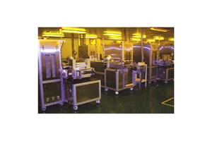
⑤ Cluster Tool Integration
⑥ Customized Software
SPECIFICATIONS
| Exposure System | ||||
|---|---|---|---|---|
| Exposure Modes | Vacuum contact | Hard contact | Soft contact | Proximity (2μ gap) |
| Advanced Beam Optics | |
|---|---|
| Uniform Beam Size | 50mm - 200mm square/round 200mm - 300 mm square/round |
| Uniformity | Better than ±3% |
| Camera | Dual Camera with CCTV with Expanded Depth of Field |
| Alignment System | |
| Pattern Recognition | Cognex visionPro¹™ with OAI customized software |
| Alignment Accuracy | 0.5μ topside 1.0μ with top to bottom optional backside alignment |
| Pre-alignment Accuracy | Better than ±50μ |
| Auto-alignme | Top to bottomside Topside |
| Wafer Handling | |
| Substrate size | 50mm – 200mm round or square or 200mm-300mm round or square |
| Thin wafers | Down to 100Μ |
| Warped Wafers | Up to 7mm-10mm |
| Thick & Bonded Substrates | Up to 7000μ |
| Robotics | Single and dual arm wafer handling |
| Run-out compensation | Standard software or optional thermal chuck |
| Wafer size conversion | 5 minutes or less |
| Throughput | 1st mask 180 wafers per hour - subsequent 75-100 wafers per hour |
| Wedge Effect Leveling | 3 point or optional non-contact |
| Available Options | |
| IR Auto-align,Cassette Mapping365nm LED Exposure Light Source Temperature Controlled Wafer Chuck Integrated Mask Management Control Integrated Lithography Cluster for Full Lithography Process Environment Control with SMIF or FOUP Interface Modules Non-contact Leveling Edge Gripping | |