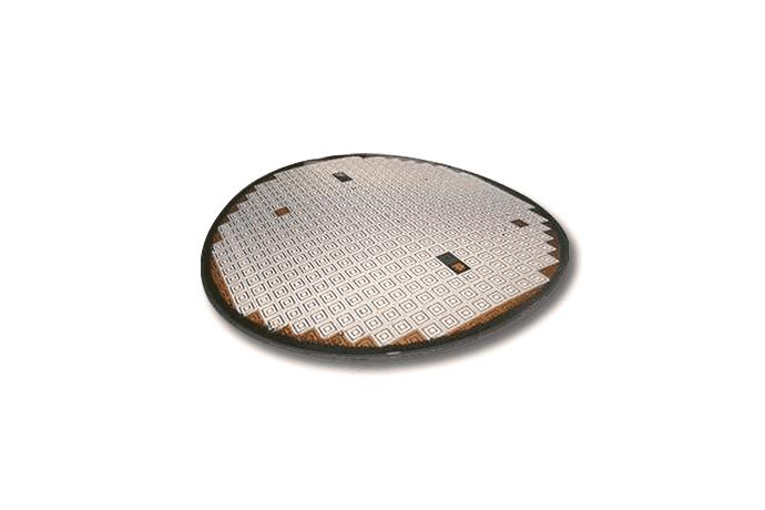
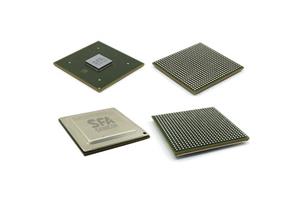
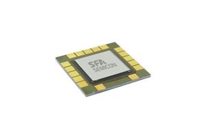
Description
On a semiconductor chip after RDL.
Fan-out structure : Some of solder balls are attached to a substrate outside of a semiconductor chip after RDL.
The process of molding the molding compound resin should be performed for Re-distribution layer which is expanded outside of chip. Additional processes for molded layer requires and turn around time is increased. The fan-out package with EMC is consequently warped due to big CTE difference after molding and package crack is generated at the interface among four different materials (Passivation, EMC Cu and Die)
Application
ㆍMobile phones (highest volume application)
ㆍDigital cameras and camcorders
ㆍMP3 players / Watch modules
ㆍLaptop and tablet computers / Medical
ㆍAutomotive
ㆍWearable electronics
Feature
ㆍReduction of TAT time with skipping WSS process.
ㆍMFG cost down & warpage improvement through using low cure polymer
ㆍNo EMC resin particle issue at sputtering process
ㆍImproved lithography techniques to compensate die shift generated at die mount process
ㆍHigh reliability performance of large sized FO-WLP


