
In case of thin film has compress stress of tensile stress, tester measures deforming rate of the board-thin film complex and calculates the residual stress.
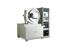
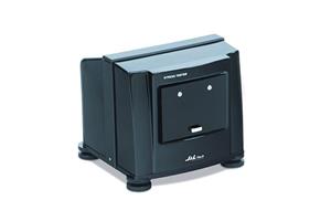
Characteristics of RESIDUAL STRESS TESTER
• Automatic control of X-Y axis
• Compute residual stress by usage of thin film's curvature Stoney formula
• (Able to measure of amorphous state)
• Easy to control
Precautions
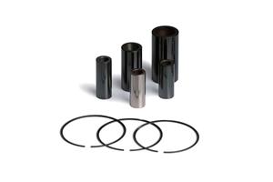
• Measuring test: Circuit board needs to use Si-wafer with 250 ± 15㎛ thickness, length better be 10 times compare to width.
• Thickness of thin film has to be slimmer than 1/50 size of circuit board.
Specification of RESIDUAL STRESS TESTER
| Range of Curvature | 2m ~ 100m | |
| Range of Measurement | 60Mpa ~ 10Gpa | |
| Resolution of Measurement | 10Mpa | |
| Range of Measurement error | < 10% | |
| Length of Maximum Scan | 30mm | |
| Stap of Minimum Scan | 0.2mm | |
| Thickness of Wafer | 100um ~ 800um | |
| Thickness of Coati ng film | 0.05um ~ 10um | |
| Scan Stage Stroke | 30mm | |
| Scan Stage Resolution | 25um | |
| Loading Stage Stroke | 140mm | |
| Loading stage Resolution | 0.5mm | |
| Speed of Measurement | 0.02mm/s | |
| Size of Test Piece | 40mm[length] x 4mm[width] | |
| Specification of PSD Sensor | 5um | |
| Device Size | 500[W] x 500[D] x 500[H] mm | |
| Weight | 30kg | |
| Power consumption | 150W | |