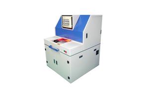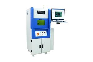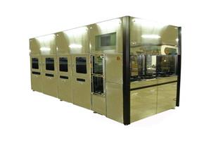
Function & Features
- Plasma를 이용한 반도체 불량 분석 장비
- ICP(Inductively Coupled Plasma) type, CCP(Capacitively Coupled Plasma) type으로 나눔
- Wafer(Silicon) 에칭, 반도체 MCP(Multi chip package)의 실리콘 다이(상층)을 에칭하여 정밀분석이 가능
- 실리콘 Layer, WBL, 다프(DAF) 에칭 가능
- 분석용도에 가장 적합한 공정조건 제공
- 다량의 시료를 동시에 작업 진행할 수 있는 챔버 시스템
- Technology
> Ion density uniformity is below 2% on 6 inch substrate
> Active substrate temperature control(He backside cooling)
> Very high etch rate
> Recipe storage and data logging
> Z-axis motion control
> Higher Uniformity by Planar ICP antenna design
> Exactly same gas conductance by unique gas diffusion gun design
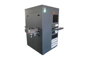
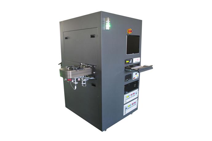
Specification(ICP type)
| Item | Description |
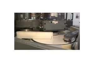
| Chamber | 1 process chamber, 1 load lock chamber with standard wafer magazines, Compact & Automatic load/lock system |
| Arm transfer | Robot arm transfer module |
| Process module | Planar type high density plasma source, Electrostatic wafer clamping with He backside cooling |
| RF System | Source 13.56MHz / 2.0 kW Bias 13.56MHz / 600 W, Auto matching network |
| Vacuum control | Auto pressure control with throttle valve |
| Gas channel | Max. 6ch Gas delivery module with mass flow controller |
| Operation | PC base control including Windows user interface for fully automatic process control |
| Dimension | 1,550(W) x 1,255(D) x 2,090(H) mm |
| Weight | Approx. 120 kg (8 inch type) |