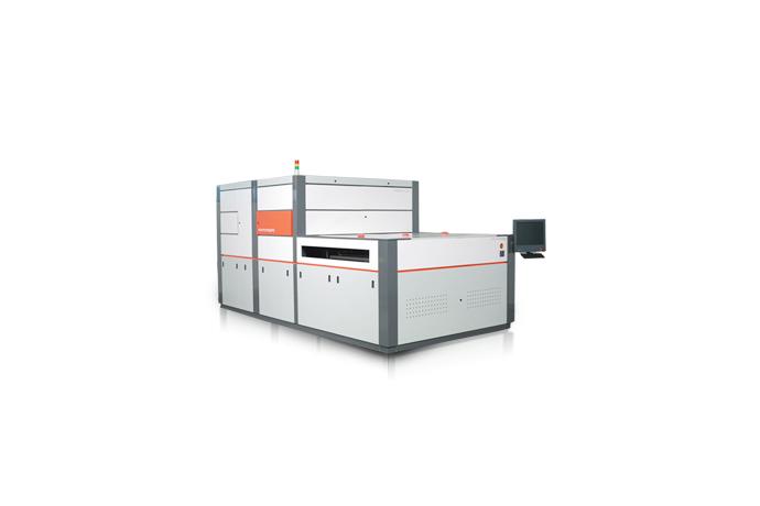
◎ Main features
- Solar Cell Thin Film Layer Laser Scribing
- Glass Size: > 5G (1100×1400) size
- Max Scribing Speed: up to 2000mm/sec
- Multi Pattern Scribing Head
- Precise Align & inspection system
◎ Main uses
- Form pattern for each layer using laser to create electrode on Thin Film Solar Cell circuit board
- Used for P1, P2, P3, P4, Edge Deletion process when manufacturing Thin Film Solar Cell
◎ Target market
- Thin Film Solar Sell (a-Si, CiS/CIGS, a-Si:H)
◎ Main technology
- Laser Beam bridging / Shaping / Delivery
- Laser Power precise control
- Optical design for high speed/precise processing
- Air Floating Stage control for high speed/precise processing
- Many equipment-related patents secured


◎ Main features
- High resolution CMOS camera measurement
- Measure number of Solar Cell and Wafer crystalline structure
- Compact & Portable Size
- Measure without removing packing box
◎ Main uses
- Measure number of crystalline structure Solar Cell, Wafer
◎ Target market
- Crystalline structure Solar Cell manufacturer
- Solar Cell wafer manufacturer
◎ Other
- Mass-production is possible for multi- crystalline structure solar cell only
- Check customer measurement safety as manufacture’s processing has significant effects on level of precision for measuring


