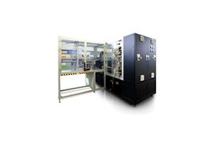

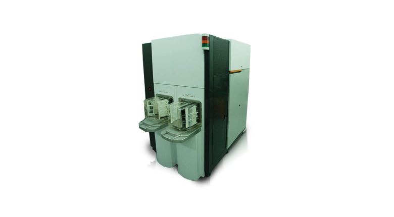


◎ Main features
- Minimize working time through Pre Aligner
- Minimize standby time through One Touch operation
- Realize various functions such as alignment, dispersion, amalgamation
- Minimize time to maintain equipment through auto tuning function of OCR
- Convenient monitoring and operation using Touch Panel
◎ Main uses
- Equipment used for WLP of semiconductor, sort processes based on wafer Unique identification mark reading wafer
◎ Target market
- Semi-conductor

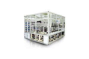
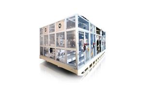
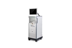
◎ Main features
- Convenient operation with user oriented design
- Maximize work efficiency using various options available
- High level of precision and stability
◎ Main uses
- Automatically pack or unpack wafer in Wafer Cassette into exclusive wafer jar box, Wafer is packed into Jar Box with Wafer Sheet by Clean Robot
◎ Target market
- Semiconductor


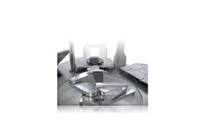
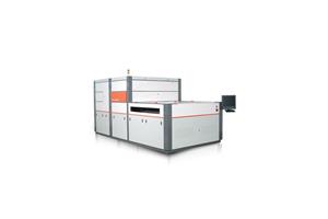
◎ Main features
- DRAM, SRAM Link-Processing
- Wafer Size : 200mm ~ 400mm
- Excellent laser processing capacity
- Precise Align & Inspection System
◎ Main uses
- Repair system to replace defective cells with spare ones by cutting links connected to them in order to save the defective chips using laser pulse through Wafer Level Test
◎ Target market
- DRAM, SRAM
◎ Main technology
- Laser Beam Shaping / Delivery
- Laser Power precise control
- Optical design for high speed/precise processing
- Air-Bearing Stage control for high speed/precise processing
◎ Main features
- Measure thickness of thin film using Reflectometry
- Materialize high speed image
- S/W to analyze 3D Imaging
- Stabilize measure and equipment
- Compact equipment
◎ Main uses
- Transparent/semi-transparent film that needs to be measured with nm thickness
- Each film thickness gauge
◎ Target market
- FPD
- Semi-conductor
- HB LED, Solar Cell
◎ Main technology
- Optical composition to measure thin film with nm thickness
- Ultra-precise measurement
- GPU high speed data treatment
◎ Main features
- Measure surface shape of thin film using Interferometry
- Materialize high speed image
- S/W to analyze 3D Imaging
- Stabilize measure and equipment
- Compact equipment
◎ Main uses
- Transparent/semi-transparent/non-transparent surface shape that needs to be measured with nm thickness
- Each surface shape gauge
◎ Target market
- FPD
- Semi-conductor
- HB LED, Solar Cell
◎ Main technology
- Optical composition to measure thin film with nm thickness
- Ultra-precise measurement
- GPU high speed data treatment