OVERVIEW
300mm semiconductor equipment of TERA obtained verified technology in the most advanced several tens nm semiconductor mass production line for heat treatment process between 100°C~1,350°C of a wide range of temperatures and CVD processes.
It can cope with all the processes up to the diffusion process and the LPCVD (Low Pressure Chemical Vapor Deposition) thin film vapor deposition process equipment.
That is, it is composed of diffusion process equipment such as thermal oxide, annealing, Cu annealing & alloying, and post baking, and LPCVD Process equipment includes (Un)Doped poly Si(P, C), LPTEOS, and Nitride and so on.
TERA provides technology with low temperature control around 100°C for mass production.
Moreover TERA’s newest technology overcomes slip which occurs during high heat treatment, (i.e. 1,200°C).
Our LPCVD equipment satisfies strict thickness uniformity and high step coverage of thin films.
This is achieved from our unique chamber structure and gas supply system.
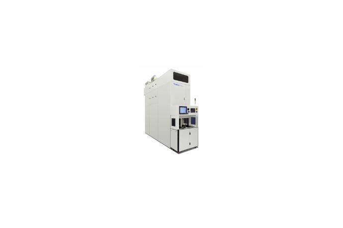
LPCVD System

The 300mm LPCVD (Low Pressure Chemical Vapor Deposition) system deposits thin film including Doped Poly Si, LPTEOS, Nitride, and MTO which is the core process for semiconductors using a chemical reaction in a low pressure state.
LPCVD is applied to several tens of nm semiconductor manufacturing process.
Moreover, it needs increased thin film uniformity and step coverage as design rules become more rigid.
Our company satisfies these specifications by our unique chamber structure and gas supply system.
And high-end equipment has excellent competitiveness which is provided by suppressing the occurrence of particles due to by-products generated through a chemical reaction, and by obtaining our company’s own design technology to prevent contamination, various mass production experiences and know-how, because of the characteristics of deposition equipment. Due to our design capability and experience, our high end equipment has excellent competitiveness by minimizing particles from by-products generated through chemical reactions which also prevent contamination.
·Applications:
- Doped Polysilicon(P, C doped Polysilicon)
- Nitride (Si3N4)
- LPTEOS, Oxide
- Radical Oxide
- ALD Oxide
·Gas delivery system with N2, Si3N4, PH3/N2, DCS, NH3, CIF3, TEOS
·CIF3 in-situ cleaning unit
·Complete chamber sealing and N2 load-lock (option)
·Flat zone: > 900mm
·100~150 product wafer per batch
·5 zones temp controller
·High speed wafer transfer robot
·16ea FOUP stock
·Full factory automation compatible
Thermal Processing

TERA provides heat treatment equipment that can be applied to various highly matured low temperature/medium temperature/high temperature heat treatment process necessary for the most advanced semiconductor mass production line within a temperature range of 100°C~1,350°C. The heat treatment system of TERA is applied to mass production at local/overseas sites of customers, in large quantities, on the basis of the thickness dispersion of verified credibility, as well as high productivity. Ultra-low temperature processing at between 100°C~400°C adopts the innovative temperature control technology of our company for uniform temperature distribution, and medium temperature equipment is mainly applied to the oxide insulating film process and each kind of annealing/flow processes.
And high temperature heat treatment equipment is divided into equipment for high temperature (1,000°C~1,200°C) and for ultra-high temperature (1,200°C~1,350°C) according to the process temperature.
Deformation (slip, warping and bowing) of wafers occurs due to thermal stress caused by high temperatures and friction stress when a 300mm wafer is treated at high temperatures of 1,000°C and over.
Patented technology to prevent the contamination of metal as well as wafer deformation is applied to equipment for high temperature in our company through the design of the optimum chamber and adjustment of air flow on the basis of ultra-precision simulation.
·Applications:
- Ultra-low temperature range(100°C~400°C): Cu anneal, Alloy, PI-Bake
- Medium temperature range(400°C~1,000°C): Thermal Oxide(Wet/Dry), Anneal & Flow
- High temperature range(1,000°C~1,350°C): Well Drive In, Densification, Thermal process for SOI & Annealed Wafer
·Complete chamber sealing and N load-lock (Option)
·Flat zone: > 900mm
·100~150 product wafers per batch
·5 zones temp controller
·High speed wafer transfer robot
·16ea FOUP stock
·Full factory automation compatible
Next Generation 450mm System


Consider the ITRS Roadmap above, it was estimated R&D of 450mm would begin in 2012.
TERA also spurs the development of 450mm vertical heat treatment equipment, and has the actual results to manufacture and deliver the world’s first 450mm chamber in the field of 450 mm vertical furnace equipment as of 2009, and obtained the final qualification about the uniformity of temperature and process results for a 450 mm heater from customers.
We do our best to develop as a leader in the 450 mm semiconductor equipment industry on this basis.


