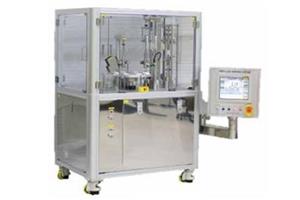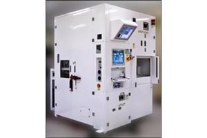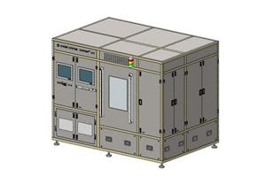


Process environment
– Substrate: 2~8 inch LED wafer
– Process environment : atmosphere
– Process : Full automation or manual loading
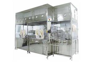
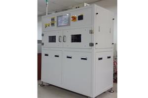
Particle treatment function
– Spin coater and cleaner
– Particle counter and suction into process area
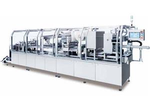
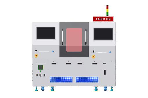
Industrial Laser & Optics for square beam
– Laser : UV ~ IR DPSS lasers
– Pulsewidth ; ns~ps, depended on performance
– Superb performance in micro-structure
– Scanner with telecentric lens
– Scan field ; 200 x 200 mm , max.
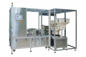
User friendly control software
– Complete automation and control solution