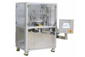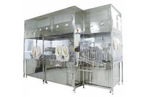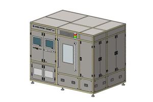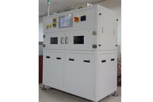
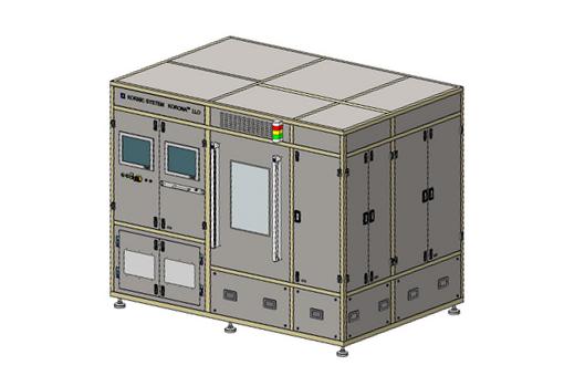
Process environment
– Substrate: 2~8 inch LED wafer
– Process environment : atmosphere
– Process : Full automation or manual loading
Various monitoring system
– Monitoring with beam profiler & energy meter
– CCD with illuminator
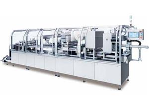
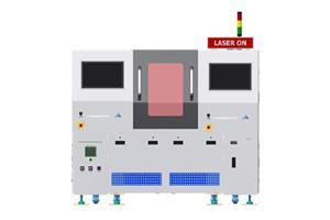
Industrial Laser & Optics for square beam
– Laser : 248 nm, 100 Hz
– Superb performance in micro-structure
– Square beam system with N2 sealed housing
– Beam size : 3 x 3 mm2, Adjustable per chip size
– Energy density at substrate : > 1.0 J/cm2
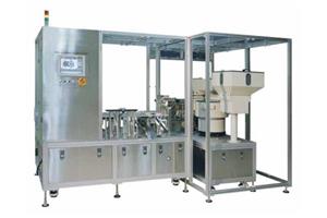
User friendly control software
– Complete automation and control solution